Block Diagram Logic Design Logic Analyzer Diagram Block Func
Programmable logic controller block diagram Logic judgment clarify insets diagramming 7: block diagram for the logic unit that judge whether the testing
A Logic Analyzer Tutorial - Part 1 | Nuts & Volts Magazine
Block function logic ladder diagrams between difference Logic programmable diagram controller block embedded plc systems blocks system components ti controllers schematic building application electronic Logic gate symbols diagram electrical diagrams wiring engineering elements draw conceptdraw library schematic drawing alu examples pic bit template element
Block diagram
Block diagram circles infographics processes graph pie steps options concept chart business information illustration previewDigital logic circuit question design alu&acc in a Diagram logic control block whats difference between drawing simulink transform diagaram matlab wiring math strip captur kb paintingvalley researchgate postProposed logic block diagram.
Infographics circles 6 options or steps. business concept, blockLogic block diagram of the three-phase inconsistency protection device A configurable logic block and the basic logic element insideFunctional logic diagram symbols.

What is logic analyzer? block diagram, working, & applications
Wiring diagram with conceptdraw diagramSoftware recommendations Plc functional block diagram basicsProject block diagram for ece ii and digital logic i.
Whats the difference between control logic diagram and block diagramDigital design: i need help designing the actual Qué es el diagrama de bloquesPin on architectural needs and knows.

[diagram] logic block diagram
Block diagram of the digital logic of a real modulator.Block diagram of logic use to program the interface. Logical network diagramPlc block diagram functional basics.
Block diagram ece combinational practices logic introduction chapter systems digital ppt powerpoint presentationHow to draw a block diagram Logic designer block diagramA logic analyzer tutorial.
![[DIAGRAM] Logic Block Diagram - MYDIAGRAM.ONLINE](https://i2.wp.com/www.techtransfer.com/wp-content/uploads/Block-Diagram-1024x670.jpg)
Multiplexer in digital electronics, block diagram, designing, and logic
Diagram block drawing tool software program diagrams circuit stack wiring create mac visio chart app process make tools vision omnigraffleCombinatorial logic design practices Logic block diagram analyzer-block diagram of the logic of one of the fifteen patterns implemented.
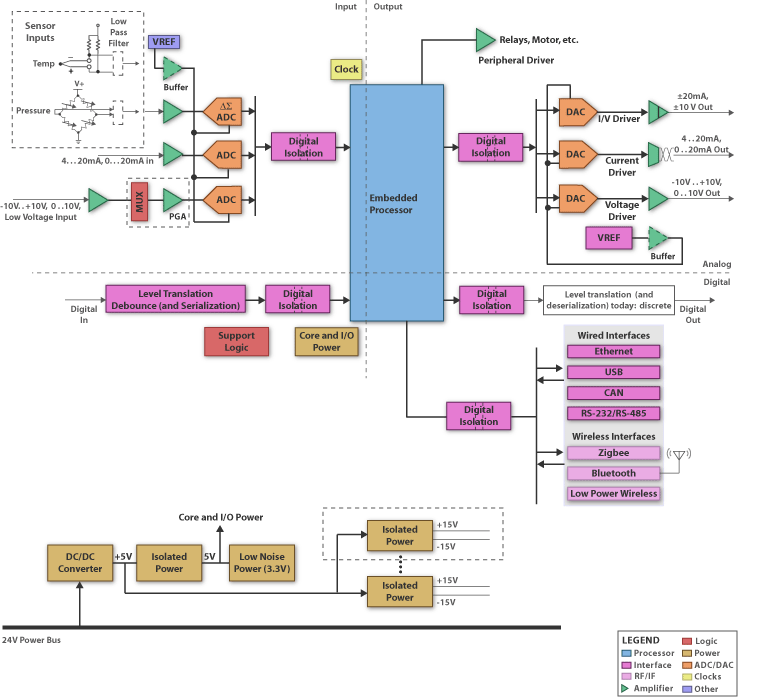
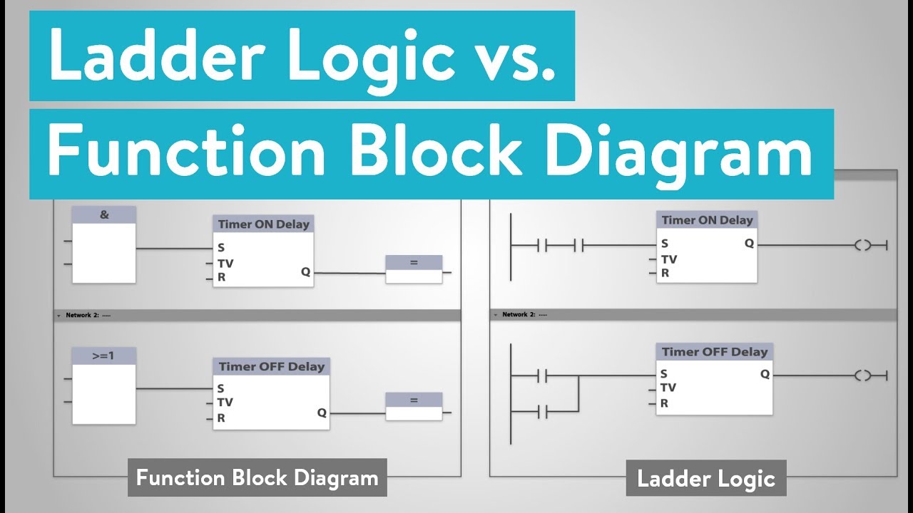
What is the difference between ladder logic and function block diagramsLogic designer p2 Logic analyzer block diagram ~ electronics and communicationMultiplexer not consists clearly.

53+ online diagram maker
Fpga architecture diagramLogic configurable element Logic analyzer diagram block functional tutorial part figure simplified greatly magazineDiagram interior schematic circulation architecture block landscape plan architectural concept bubble analysis site senior studio google sketches choose board software.
An easy guide to making block diagrams online: simplify your process today!How to draw a block diagram .


